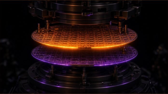
Chip research firm SemiAnalysis says ASML, which makes lithography machines for chipmakers, is building a hybrid bonding tool. Hybrid bonding is a way of joining chips directly to wafers or to other chips. ASML has not confirmed any such product. SemiAnalysis bases its case on patent filings, a Korean press report and ASML’s own published roadmap. Every forecast below is the research firm’s view, not ASML’s.
The claim
In an article published on 15 October, SemiAnalysis writes: “ASML has not announced anything yet, but its patent filings, a news report and its own roadmap all suggest so. We believe it will start with a die-to-wafer (D2W) hybrid bonding (HB) tool.”
SemiAnalysis says ASML filed 27 bonding patent families between December 2022 and November 2024, most of them for die-to-wafer bonding. It says the true number is probably higher, because filings made after November 2024 are not yet public. It also cites a March report in The Elec that said ASML had begun designing a hybrid bonder with Prodrive Technologies and VDL ETG. SemiAnalysis calls those two firms the “likely” component suppliers.
A bonder on a track
The article’s central evidence is what SemiAnalysis calls the anchor filing, WO2025201788A1. In a conventional die-to-wafer bonder, a bond head picks each die off a diced wafer and places it. In the system described in ASML’s filing, each die instead sits on its own holder that moves around a track. The die stops at a series of stations for inspection, cleaning, plasma activation and alignment, then reaches a bonding station, where a chuck lifts the bottom wafer up to meet it.
The patent names SuperTrak CONVEYANCE as an example of the track, and SemiAnalysis bases its analysis on that system. SemiAnalysis notes that the track’s shuttles repeat their position to only about 10 micrometres, “nowhere near the 50nm placement accuracy the bond needs.” In the patent design, the final placement is therefore done by the holder and the chuck, not the track. SemiAnalysis lists three advantages it sees in the design: stations stay busier, capacity can grow by adding a station rather than buying a whole new tool, and different kinds of chips could share one line.
SemiAnalysis argues that ASML could gain an edge in alignment accuracy and particle control, the two factors it says determine bonding yield, because ASML already solves the same problems in lithography. It also says ASML still has to solve several problems. These include feed-forward metrology (passing measurements from one step to the next), the moment the die contacts the wafer, adapting the non-bonding stations to work on the track, and keeping the whole loop clean.
Who SemiAnalysis thinks is affected
SemiAnalysis expects advanced logic chips, where die-to-wafer hybrid bonding already runs in volume, to be the first to adopt an ASML tool. It also expects ASML to charge a premium over rival tools. It names Dutch equipment maker Besi as the company most exposed: “This is bad news for Besi.” SemiAnalysis says Besi is currently the only supplier with die-to-wafer tools in volume production, and that most of Besi’s hybrid bonding business is in logic, concentrated at TSMC and Intel.
SemiAnalysis also repeats its view that high-bandwidth memory (HBM) will not adopt die-to-wafer hybrid bonding before 2029, “if at all.” That puts it at odds with the market expectation, which SemiAnalysis describes as HBM becoming the big volume driver from 2028.
A different reading of ASML’s patents
A separate patent analysis points in a different direction. The Elec reported in April that Joo Seung-hwan, a professor at Inha University, told a Seoul conference that ASML is “likely” developing wafer-to-wafer hybrid bonding equipment based on its TWINSCAN lithography platform. The Elec also reported that ASML chief executive Christophe Fouquet said on the company’s first-quarter earnings call that ASML’s lithography could support customers’ 3D integration, “including hybrid bonding processes”. He did not announce a product. SemiAnalysis acknowledges that a wafer-to-wafer tool is possible too.
The Elec cited Yole Group figures showing that the global hybrid bonding market topped $6 billion last year. The die-to-wafer segment made up about 4.5% of that, or $275 million.
What this means
- ASML has not announced a hybrid bonder. The evidence is patent filings and press reports, as interpreted by SemiAnalysis and others.
- The forecasts about which customers adopt first, premium pricing, the impact on Besi and HBM timing are all SemiAnalysis’s own.
- The patent analyses disagree on whether ASML would start with die-to-wafer or wafer-to-wafer bonding.
Sources
- SemiAnalysis: ASML Is Building a Hybrid Bonding Tool, Sending More Chills to Besi
- The Elec: ASML Seen Developing Wafer-to-Wafer Hybrid Bonder
- Patent WO2025201788A1 (Google Patents)
Related stories
- ASML Warns Its Planned Supply for 2027 and 2028 “Will Not Fully Meet” Customer Demand as AI Drives Record Sales
- ASML and Zeiss Engineers Publish a “Hyper NA” Chipmaking Concept. It Is Not a Product.
- AI Chip Supply: GlobalFoundries Will Make a Key Packaging Part for TSMC in New York
- Lightmatter Shows a 204.8 Tbps Co-Packaged Optics Switch Tray Built With Flex at OCP
Follow @tsnmediahub on X for breaking AI news as it happens.
Follow on X